
High-Speed Wafer Positioning System for Inkjet Cartridge Manufacturing

Problem
A machine builder had designed a wafer inspection system to catch defects in silicon wafers used to manufacture inkjet printer cartridges, but had no way to control the motion. Each wafer required positioning and scanning at 100-nanometer resolution, at production throughput, with the flexibility to inspect either every die on the wafer or a statistical sample.

Solution
AMS engineered the full motion control system: a three-axis stage and camera positioning architecture with interpolated moves to compensate for wafer misalignment, a high-speed dual-ported RAM interface to receive inspection instructions from the host computer, and a triggering architecture that fired the camera at precise, sub-micron position intervals so line-scan images could be reconstructed on the fly.

Result
The architecture proved robust enough that the customer built a product line around it: approximately six inspection systems, deployed across a global printer manufacturer’s facilities on multiple continents.
The Problem: Inspecting a Wafer Fast Enough to Keep Up With Production
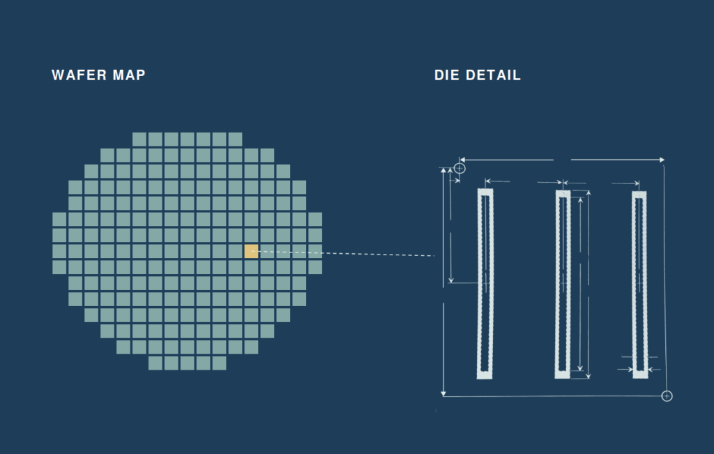
A machine builder was developing a wafer inspection and measurement system for a customer that manufactured thermal inkjet printer cartridges. Each silicon wafer coming off the line held 256 individual dies, and each die contained three micro-sandblasted slots that would become the ink chambers inside a finished cartridge, with zero tolerance for defects that would compromise print head performance.
Production throughput required inspecting these wafers at production speed. Depending on the quality plan, that meant either full inspection of all 256 dies or a statistical sample covering a subset. Either way, the wafer had to be positioned beneath a line-scan camera at 100-nanometer resolution, with image capture triggered precisely enough that the scan lines could be reconstructed into a complete image of each micro-machined slot.
The customer had already resolved the mechanical architecture: the XY stage, linear motors, and camera. What remained unsolved was precision motion control, along with a data path capable of moving inspection instructions from the host computer to the hardware at production speed.
The ask: a motion control system capable of positioning a wafer to within a fraction of a micron, on demand, at the speed that the production inspection schedule required.
The Solution: A High-Speed Interface, a Trigger Architecture, and Interpolated Motion
Getting Instructions to the Hardware
The inspection parameters, which determined which dies to sample and in what sequence, resided on a host computer. AMS configured a high-speed dual-ported RAM interface to transmit that data, along with command and status information, into a Delta Tau PMAC motion controller allowing high speed data exchange without slowing the inspection cycle. The controller translated those parameters into coordinated motion: positioning the wafer under the camera, adjusting focal height on a third axis, and, when a wafer wasn’t seated squarely on the table, compensating through camera rotation on a fourth axis and interpolated X-Y moves to keep the scan path aligned with each slot.
Synchronizing Capture With Motion
The harder problem was synchronization. The system ran on a Delta Tau PMAC motion controller, and AMS configured the triggering logic around a compare-equals-output function: a feature that fires a digital output at a specified position and then auto-increments the trigger point by a fixed interval, such as every half micron, without additional computation between cycles. This signal fed directly into the camera’s image acquisition trigger system, telling it exactly when to capture its next 255-pixel-wide scan line, and into the video board, instructing it to append that line to the image already in progress. The wafer stayed in continuous motion throughout; the image was assembled one line at a time, at whatever resolution the inspection called for.
A Data Architecture Borrowed From an Unrelated Industry
The dual-ported RAM interface wasn’t built for this application originally. It came from an earlier project: streaming positional data to a five-axis milling machine cutting tooling for fiberglass boat hull molds. Different industry, different customer, same underlying constraint: moving high-bandwidth positional data in real time. It’s the case for treating motion control as a transferable engineering discipline rather than an industry-specific one; the same architectural problem surfaces in a marine tooling shop and a semiconductor fab, and the same solution applies.
The customer retained ownership of the stage, camera, and mechanical design. AMS’s scope covered motion control, encoder feedback design, servo drives, and the operator interface: the control layer that made the mechanical concept operational.
The Results: A Product Line, Not Just a Single System
The system met its inspection specification and became the basis for a product line. The customer went on to build and sell additional inspection systems on this architecture, deployed across the manufacturer’s facilities in multiple locations, including Singapore and Oregon.
Outcomes by Category
A functional architecture where none had existed. The customer had a mechanical concept and no path to control it. AMS delivered the interface and control architecture that made the concept operational.
The design scaled into a product line. What began as a single inspection system became a standard product offering, deployed across the customer’s global manufacturing footprint on the same core motion control architecture.
Production-grade inspection speed at sub-micron resolution. The compare-equals-output triggering architecture allowed continuous image capture and reconstruction at a resolution fine enough to catch defects in a 100-nanometer-tolerance manufacturing process, without interrupting wafer motion.
Cross-industry pattern recognition remains core to AMS’s engineering approach. The dual-ported RAM architecture originated on a marine tooling project with no apparent connection to semiconductors. Recognizing the underlying architectural equivalence is the kind of reasoning AMS applies to every new engagement.
About Applied Motion Systems
AMS is a systems integrator and machine builder working in motion control and industrial automation, across glass container manufacturing, paper converting, aerospace tooling, and applications most companies haven’t attempted. This was one of the earliest semiconductor projects AMS undertook, and semiconductor manufacturing has remained part of our work since.
If you’re facing a motion control or automation problem without an obvious solution, we’d welcome the opportunity to look at it with you.
Key Takeaways
- The customer had the mechanical concept but no path to control it. AMS engineered the motion control system from the ground up: four-axis positioning, encoder feedback, drives, and the operator interface.
- Sub-micron precision required more than fast hardware; it required a synchronization architecture. The compare-equals-output function on the Delta Tau PMAC controller triggered the camera automatically at fixed position increments, enabling continuous image capture and reconstruction during wafer motion.
- A high-speed dual-ported RAM interface moved inspection instructions from the host computer to the controller without introducing latency, built on architecture developed for an unrelated application in a different industry entirely.
- A single system became a product line. The customer built and sold numerous units of the design, deployed across production facilities in multiple countries.
Start the Conversation
All of our collaborations begin with an open dialogue.
More Case Studies
Industry
Technology