
Semiconductor Automation Integration
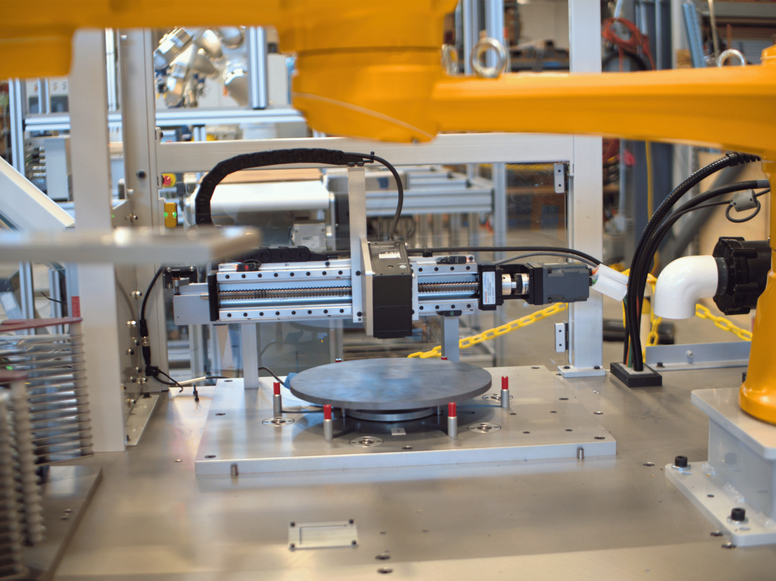
Semiconductor manufacturing operates at a level of precision and cleanliness that most industries never encounter. The machines that measure, mark, and handle wafers often achieve tolerances measured in microns, and in some cases nanometers. AMS has worked in semiconductor manufacturing since our early years, designing and integrating custom motion control systems and equipment for applications where off-the-shelf solutions don’t exist and the tolerance for error is effectively zero. Our work in this space spans precision positioning, wafer inspection and measurement, custom end-of-arm tooling, and the integration of multiple control platforms and plant communication protocols. We bring the same engineering-first approach to the semiconductor industry that we apply across every industry we serve: understand the machine, the environment, and the people who operate it before specifying anything.
What We Do in Semiconductor
Precision Motion Control and Positioning
Many semiconductor applications demand motion control and coordination that most standard systems aren’t capable of. In a recent project, the machine measures wafer flatness, laser-marks individual samples for permanent identification, and pre-aligns wafers ranging from 200mm to 300mm in diameter, with thicknesses from 1mm to 11mm, without a physical changeover between sizes. The pre-alignment system, which centers and clocks each wafer to a notch or flat edge feature before marking, had no off-the-shelf solution that covered the full range. We designed our own.
Custom End-of-Arm Tooling
Handling wafers at production weights ranging from 50 grams to 1.8kg without a tool change requires tooling that can grip without damaging, place the heavier wafers into cassettes without sagging, and position the range of wafer sizes at each operation in the cell accurately and reliably. We carry lessons learned from one machine to the next. On this project, we designed a custom vacuum end-effector using 3D-printed TPU suction cups to achieve a reliable grip across the full range of wafer sizes and weights. The result was robust enough that the customer asked us to design additional vacuum cups for other machines in their facility.
Multi-Generation Plant Integration
Modern semiconductor facilities rarely operate on a single generation of control software. In one recent project, a wafer-processing cell needed to interface with two distinct plant control systems: one supporting 300 mm wafer production and another supporting 200 mm operations. Because the facility maintains full traceability for every wafer, sample, and crystal lot throughout the manufacturing process, the equipment had to exchange accurate, timely data with both systems at every relevant process step.
Achieving this integration required more than configuring motion control. It required an early understanding of each system’s data model, traceability requirements, communication protocols, and operational workflows. The two networks used different protocols and interface expectations, so the communications software became a primary focus during project discovery and design. Addressing those requirements upfront reduced integration risk, protected lot-tracking continuity, and helped ensure a smooth installation and commissioning process.
Legacy System Modernization
Some of the most important machines in a semiconductor facility are also the oldest. In a recent project, we replaced equipment that had been in service for over 20 years, running on Japanese-language documentation, supported only by vendors overseas, and no longer able to handle current-generation wafer sizes. We provided English-language documentation and the engineering depth to take over where the original manufacturer left off.
Platform Expertise
AMS works with the platforms our customers’ facilities already use and brings informed recommendations when a new build gives us the latitude to specify.
- Siemens PLC – Deployed in semiconductor applications where design flexibility and cross-system communication are priorities.
- Stäubli Robotics – Integrated for precision wafer handling applications requiring reliable grip and repeatable positioning across variable wafer sizes and weights.
- Keyence – Sensing and measurement components across semiconductor applications.
- Balluff I/O – Deployed in semiconductor integration work, with strong vendor support throughout.
How We Work
Every AMS engagement begins the same way: we look at the machine and production requirements, talk to the people who run it, and ask why it’s doing what it’s doing and what could be improved. In the semiconductor industry, this discovery process is more consequential than in most industries. The tolerance for a mismatch between what we specify and what the production environment demands is effectively zero.
We don’t design around a proprietary platform or a preferred solution we’re trying to place. When our customer gave us more freedom on a second machine after a successful launch of serial #1, we chose differently, and the results showed it. When a standard component doesn’t exist for the range of wafers we needed to handle, we designed one.
We also design for the people operating the machine every shift and focus on operator and technical training for a definitive technology transfer to those who will own the machine going forward. Clear operator interfaces, English-language documentation, and systems that your in-house team can troubleshoot without needing to call us are part of what and how we build.
Key Takeaways
- AMS designs custom motion control systems for semiconductor applications where off-the-shelf solutions don’t exist, including pre-alignment systems built to handle multiple wafer generations without physical changeover requirements.
- When a standard component doesn’t cover the range that the application requires, AMS engineers it from scratch, including end-of-arm tooling designed for precision grip across wafer sizes from 200mm and 50 grams to 300mm at 1.8 kg.
- AMS integrates across multiple generations of plant control software, designing machines that communicate with the facility’s existing network systems in a well-documented, reliable fashion.
- We work with the platforms that perform best for the application and bring informed recommendations when a new build gives us the latitude to specify.
- Semiconductor customers come to AMS when they’re fighting obsolescence, losing access to overseas support, or working with systems that were never quite right. We take over where the original manufacturer left off and build something meant to last another 20 years.
Tell Us About Your Machine
If you’re running semiconductor manufacturing equipment that’s aging out, communicating across generations of plant software, or requiring precision your current integration partner hasn’t been able to deliver, we’d welcome a conversation.