
Enabling a mix of 200mm – 300mm Wafer Production With a Single Locally Supportable Automation Platform

Problem
A semiconductor producer’s legacy Japanese-supplied equipment measured, aligned, and marked wafers up to 200mm in diameter and 1mm thick. A planned migration to 300mm wafers up to 12mm thick introduced payload and precision requirements no off-the-shelf pre-aligner or wafer-handling robot could accommodate, on a platform that also created documentation and support challenges for the North American factory.

Solution
AMS developed a custom six-bar-linkage pre-aligner and 3D-printed flexible-vacuum-cup end-of-arm tool that handled both 200mm and 300mm wafers without physical changeover, replacing the legacy controls and wafer-handling platform with a Siemens PLC and Stäubli robotic arm. Dual-protocol communications let the cell operate with two concurrent generations of wafers and plant-control software throughout the customer’s transition.

Result
A single machine now processes both legacy and current wafer generations without physical changeover. Supported by English-language documentation and local technical resources, the Siemens-based control platform has since been adopted by the customer as its new standard specification.
How Applied Motion Systems built a single system that measures, aligns, marks, and handles both 200mm and 300mm silicon wafers, with no changeover between sizes
Overview
Applied Motion Systems (AMS) was engaged by a global semiconductor wafer manufacturer to develop a next-generation wafer measurement, alignment, and marking system. The system needed to support the industry’s current 300 mm wafer format while continuing to process legacy 200 mm wafers on the same platform, without manual tooling changes or physical reconfiguration between wafer sizes.
The manufacturer, an early high-volume producer of 300 mm wafers with a significant share of global wafer production, relied on Japanese OEM equipment that had been in service for more than two decades. Although the legacy system supported earlier wafer generations, its Japanese-language documentation and remote support model complicated local sustainment. It also lacked the mechanical capacity, handling flexibility, and control-system compatibility needed to reliably process the larger, thicker 300 mm wafers and communicate with the manufacturer’s evolving plant-control environment.
The Problem
Precision and Traceability Requirements
The system measures, aligns, and marks every wafer before downstream processing. It captures wafer thickness at five locations with micron-level resolution and calculates total thickness variation (TTV) as the difference between the maximum and minimum readings. This measurement serves as both a product-quality check and an early indicator of upstream tool condition. As crystal-cutting tools wear, variation across sampled wafers increases before other failure signatures appear.
The system also laser-marks sampled wafers with a permanent process identifier. The mark must remain legible after subsequent surface grinding, since engineers periodically retrieve and remeasure selected wafers, sometimes years after initial processing, to assess long-term process performance.
Dimensional and Payload Range
The primary engineering challenge was the required dimensional and payload envelope. Production wafers ranged from approximately 50g to 1.8kg, depending on diameter and thickness. At the upper end, the payload exceeded the capacity of conventional semiconductor pre-alignment equipment. Pre-aligners are mature, high-volume products, but commercial units are generally designed around a defined wafer diameter, thickness, and payload range. No available system could accommodate the manufacturer’s full 200mm-to-300mm diameter range and complete production-thickness range on one platform.
Dual Plant-Control Integration
Control architecture introduced a second constraint. The manufacturer’s plant network performs automated part, lot, and crystal tracking across the entire production flow, eliminating manual sample logging at the operator level. That tracking infrastructure exists as two discrete systems: one governing 200mm production, one governing 300mm. A unified platform needed to interface reliably with both concurrently.
Moving Beyond the Legacy Platform
AMS built the manufacturer’s prior machine to its specification, including PLC and robot selection, and supported it under the same overseas documentation model. The platform performed well, but the customer wanted the next design cycle to move toward a more supportable, English-language, locally accessible automation standard, built around control and robotic components it intended to standardize across future equipment.
The Solution
Custom Pre-Aligner Design
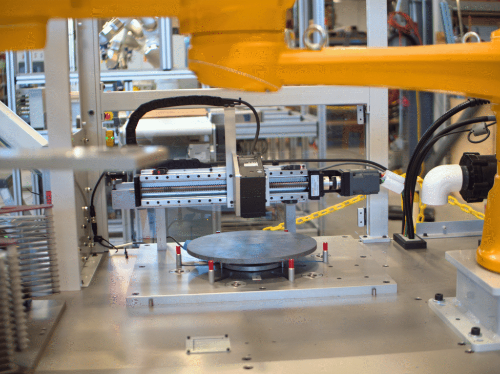
AMS designed and fabricated a custom six-bar-linkage pre-aligner to center each wafer before edge-notch and defect detection, then clock it into position for laser-mark placement. The system used 3D laser profiling to detect the wafer edge and notch position, then rotated the wafer to the required orientation for marking. No commercially available pre-aligner covered the required combination of 200mm-to-300mm wafer diameters, full production thickness range, and maximum payload, so the pre-aligner became the project’s principal custom-engineering deliverable.
Custom End-of-Arm Tooling
End-of-arm tooling introduced a related challenge. The tool had to remain rigid enough to prevent deflection at maximum payload and precise enough to protect quality-critical samples during load and unload. It also needed compliant contact surfaces to avoid surface marking during transfer. Building on lessons from its earlier machine for the customer, AMS developed a custom vacuum-cup end effector using additively manufactured flexible TPU cups. The design reduced end-effector mass while conforming across the full wafer-size range without physical tool changes, and its performance led the customer to request additional custom vacuum-cup designs for other equipment in the facility.
Controls and Hardware Platform
For the control system and wafer-handling architecture, AMS proposed a Siemens PLC and Stäubli robotic arm to replace the prior platform. The HMI managed operator interaction, machine status, alarms, recipes, and communication with the factory network systems. Keyence laser-profiling equipment supported wafer-edge measurement, notch detection, and orientation functions, while a Keyence laser-marking system applied the permanent process identifier. Balluff I/O hardware streamlined the connection of machine sensors, bar code readers, and actuators to the control system.
Dual-Protocol Plant Communication
This architecture represented the customer’s first departure from the incumbent control and robot platform for this class of equipment, driven by AMS’s Siemens integration experience. To support both wafer generations throughout the transition, AMS engineered a dual-protocol communication capability that let the system interface with the 200mm and 300mm plant-tracking networks simultaneously. The result eliminated the need for separate dedicated machines or physical reconfiguration between wafer generations.
The Outcome
A single platform now processes both current and legacy wafer generations without physical changeover. Previously, supporting multiple wafer sizes required dedicated primary and backup machines for each wafer generation, or manual reconfiguration such as installing an 8 mm pre-alignment stage. The consolidated architecture allows any compatible unit in the customer’s fleet to provide backup capacity for another, reducing dependence on generation-specific equipment and improving operational flexibility.
The customer’s engineering team characterized the Siemens-based control platform as a substantial improvement over its prior standard and subsequently adopted it as the default specification for future equipment. English-language documentation and U.S.-based technical support further reduce the manufacturer’s reliance on overseas resources for equipment operating in its North American facilities.
From Applied Motion Systems
“Our strong understanding of our customer’s process and our relationship with Siemens allowed us to deliver something elegant. A unified solution that handles both 200mm and 300mm wafers across multiple thicknesses, deployable across multiple plant locations with consistent throughput and reliability. We delight in providing these types of innovative solutions to our customers.”
— Bruce Hagerty, Chief Growth Officer, Applied Motion Systems
From Siemens
“AMS demonstrated exceptional innovation in developing a solution capable of handling larger and heavier wafers while maintaining the precision required in semiconductor manufacturing. Siemens was proud to provide the automation and motion platform that helped enable a flexible, autonomous, and fully integrated solution for the customer.”
— Brian Taylor, Head of Semiconductors, Siemens Digital Industries US
Technologies
- Custom six-bar-linkage pre-aligner spanning 200mm to 300mm wafer diameters
- Additively manufactured TPU vacuum-cup end-of-arm tooling
- Siemens PLC and servo drive platform
- Stäubli robotic arm for wafer handling
- Keyence laser profiling and etching systems
- Balluff I/O
- Concurrent dual-network plant communication across two software generations
About Applied Motion Systems
AMS is a systems integrator and machine builder. Our work spans motion control and industrial automation across glass containers, paper converting, forest products, aerospace tooling, renewable energy, semiconductor wafer processing, and applications most companies haven’t attempted.
We begin every engagement by characterizing the process: the machine, the material, the operating environment, and the constraints governing system performance. We design for the environment the system will operate in, and for its performance years after commissioning, since that horizon is where design quality becomes evident.
Key Takeaways
- Legacy equipment was constrained to 200mm wafers and 1mm thickness. Migration to 300mm wafers, up to 1.8kg at maximum payload, exceeded the load and precision capacity of any commercially available pre-aligner or wafer-handling robot.
- No commercial pre-aligner spanned the required dimensional envelope. AMS engineered a custom six-bar-linkage pre-aligner to center and clock wafers from 200mm to 300mm in diameter across the full production thickness range.
- Additively manufactured TPU vacuum cups resolved the end-of-arm tooling constraint, gripping maximum-payload wafers without deflection or surface damage, at a performance level that led the customer to commission additional cup designs for other equipment.
- The platform interfaces concurrently with two generations of plant tracking software, eliminating manual sample tracking across wafer generations.
- AMS specified Siemens and Stäubli in place of the customer’s incumbent PLC and robot platform, the customer’s first deviation from standard specification for this equipment class, informed by prior integration experience.
- Net result: a single platform, zero changeover, and domestic English-language support, replacing a model requiring dedicated primary and backup hardware per wafer generation and overseas vendor support.
Start the Conversation
All of our collaborations begin with an open dialogue.
More Case Studies
Industry
Technology